
Implementation of integrated circuit and design of SAR ADC for fully implantable hearing aids
Abstract
BACKGOUND:
The hearing impaired population has been increasing; many people suffer from hearing problems. To deal with this difficulty, various types of hearing aids are being rapidly developed. In particular, fully implantable hearing aids are being actively studied to improve the performance of existing hearing aids and to reduce the stigma of hearing loss patients. It has to be of small size and low-power consumption for easy implantation and long-term use.
OBJECTIVE:
The objective of the study was to implement a small size and low-power consumption successive approximation register analog-to-digital converter (SAR ADC) for fully implantable hearing aids.
METHODS:
The ADC was selected as the SAR ADC because its analog circuit components are less required by the feedback circuit of the SAR ADC than the sigma-delta ADC which is conventionally used in hearing aids, and it has advantages in the area and power consumption. So, the circuit of SAR ADC is designed considering the speech region of humans because the objective is to deliver the speech signals of humans to hearing loss patients. If the switch of sample and hold works in the on/off positions, the charge injection and clock feedthrough are produced by a parasitic capacitor. These problems affect the linearity of the hold voltage, and as a result, an error of the bit conversion is generated. In order to solve the problem, a CMOS switch that consists of NMOS and PMOS was used, and it reduces the charge injection because the charge carriers in the NMOS and PMOS have inversed polarity. So, 16 bit conversion is performed before the occurrence of the Least Significant Bit (LSB) error. In order to minimize the offset voltage and power consumption of the designed comparator, we designed a preamplifier with current mirror. Therefore, the power consumption was reduced by the power control switch used in the comparator.
RESULTS:
The layout of the designed SAR ADC was performed by Virtuoso Layout Editor (Cadence, USA). In the layout result, the size of the designed SAR ADC occupied 124.9
CONCLUSIONS:
We proposed a low-power 16-bit 32 kHz SAR ADC for fully implantable hearing aids. The manufactured SAR ADC based on this design was confirmed to have advantages in power consumption and size through the comparison with the conventional ADC. Therefore, the manufactured SAR ADC is expected to be used in the implantable medical device field and speech signal processing field, which require small size and low power consumption.
1.Introduction
Recently, the hearing impaired population has been increasing continuously and many people suffer from hearing problems. To deal with this problem, various types of hearing aids are being rapidly developed. In particular, fully implantable hearing aids are being actively studied to improve the performance of existing hearing aids and to reduce the stigma of hearing loss patients [1, 3].
Fully implantable hearing aids consist of an implantable microphone, signal processor, and vibrational transducer. An analog-to-digital converter (ADC) is the first step of the signal processor to convert an input analog signal to a digital signal suitable for signal processing. In addition, the ADC in the signal processor requires small size and low power consumption for easy implantation and long-term use. Prior to the design of the ADC, the sampling frequency and the resolution of the ADC were selected by considering the characteristics of the fully implantable hearing aid. Among various types of ADC methods,
In this paper, we designed a small sized and low-power-consumption SAR ADC for fully implantable hearing aids. The designed SAR ADC consists of sample and hold, a voltage follower, comparator, R-2R ladder digital-to-analog converter (DAC), and SAR logic. The small size and low power consumption are achieved by a DAC based on an R-2R resistor array and comparator using power control switches and, offset rejection techniques. The simulation results show that a reference voltage was approximated to the sampled value of the input signal. The SAR ADC is implemented in SMIC 180 nm CMOS technology. The total power consumption is 50
2.Method
2.1Considerations for design of ADC for fully implantable hearing aids
The audible range of humans is a frequency range of 20–20,000 Hz, as shown in Fig. 1 [6, 7]. The area of interest of ADC design is a speech range with a frequency range of 100–8,000 Hz. The characteristics for each frequency band are shown in Table 1, and 500–4,000 Hz with speech intelligibility of 83% in the speech area is important [8]. Therefore, a sampling frequency of 32 kHz for speech signal processing based on the Nyquist theory is selected. In order to determine the resolution of the ADC, in accordance with the distinguishable quality of the minimum sound pressure level in the speech area, we considered the operating characteristics and dynamic range of an implantable microphone. The implantable microphone operating characteristics are shown in Fig. 2. The microphone output signal was amplified to 25 dB to meet the input voltage range of the designed ADC. Because the 25 dB amplified 50 mV ac peak signal became an 889 mV ac peak signal, to avoid half wave clipping, the ADC needed an input bias voltage of 900 mV, which is the closest voltage to 889 mV. For the 1.8 v driven ADC, the LSB resolution of the 16 bit ADC is 27.46
Table 1
Speech intelligibility for each frequency band
| Speech frequency [Hz] | Speech intelligibility [%] |
|---|---|
| 100–500 | 5 |
| 500–1,000 | 35 |
| 1,000–2,000 | 35 |
| 2,000–4,000 | 13 |
| 4,000–8,000 | 2 |
Figure 1.
Graph of audible range.
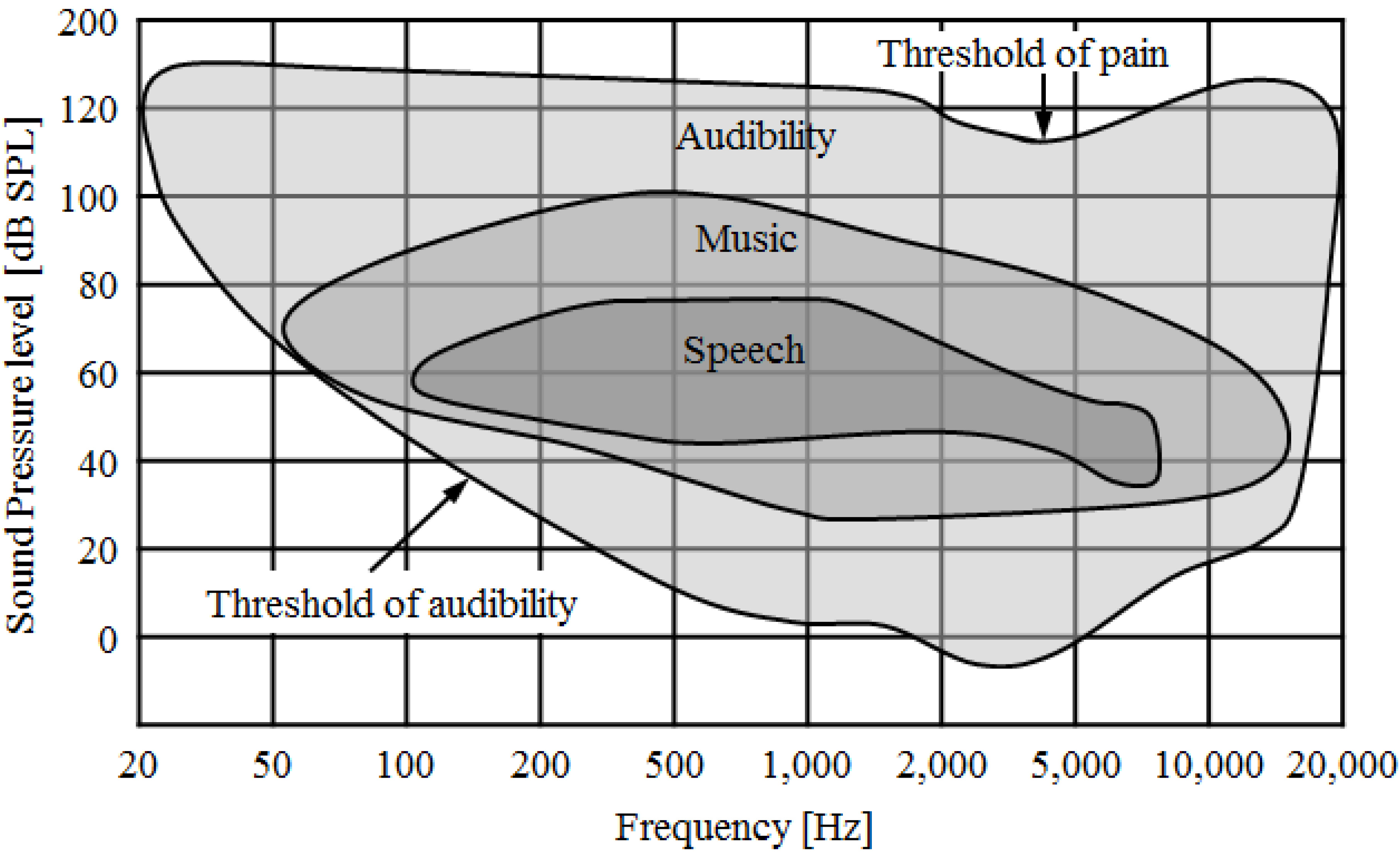
Figure 2.
Operating characteristics of implantable microphone.
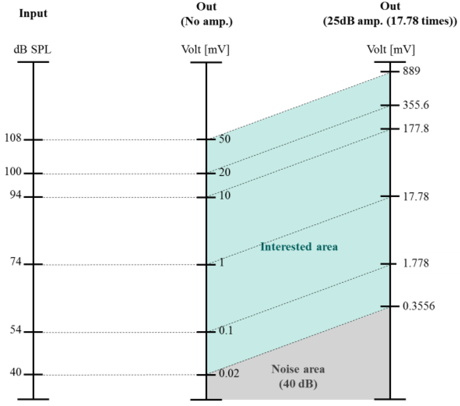
Figure 3.
Minimum sound pressure level of each bit to distinguish speech regions.
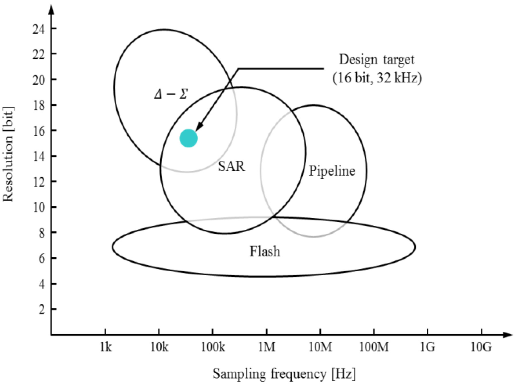
The speech and audio application fields generally require a high resolution and slow conversion speed. Therefore, the design target of ADC for fully implantable hearing aids was determined to be 16 bit and 32 kHz. The structure of a typical ADC in accordance with the resolution and conversion speed is shown in Fig. 3, and the ADC structure of advantages and disadvantages according to Fig. 3 is shown in Table 2 [9]. As shown in Fig. 3 and Table 2, the SAR ADC and
Table 2
Advantages & disadvantages of ADC architecture
| Structure | Advantage | Disadvantage |
|---|---|---|
| Flash | High speed & latency | Size & resolution & power |
| Pipeline | Speed | Latency |
| SAR | Power & size | Speed |
| Delta-sigma | Resolution | Latency & speed |
2.2Design of SAR ADC
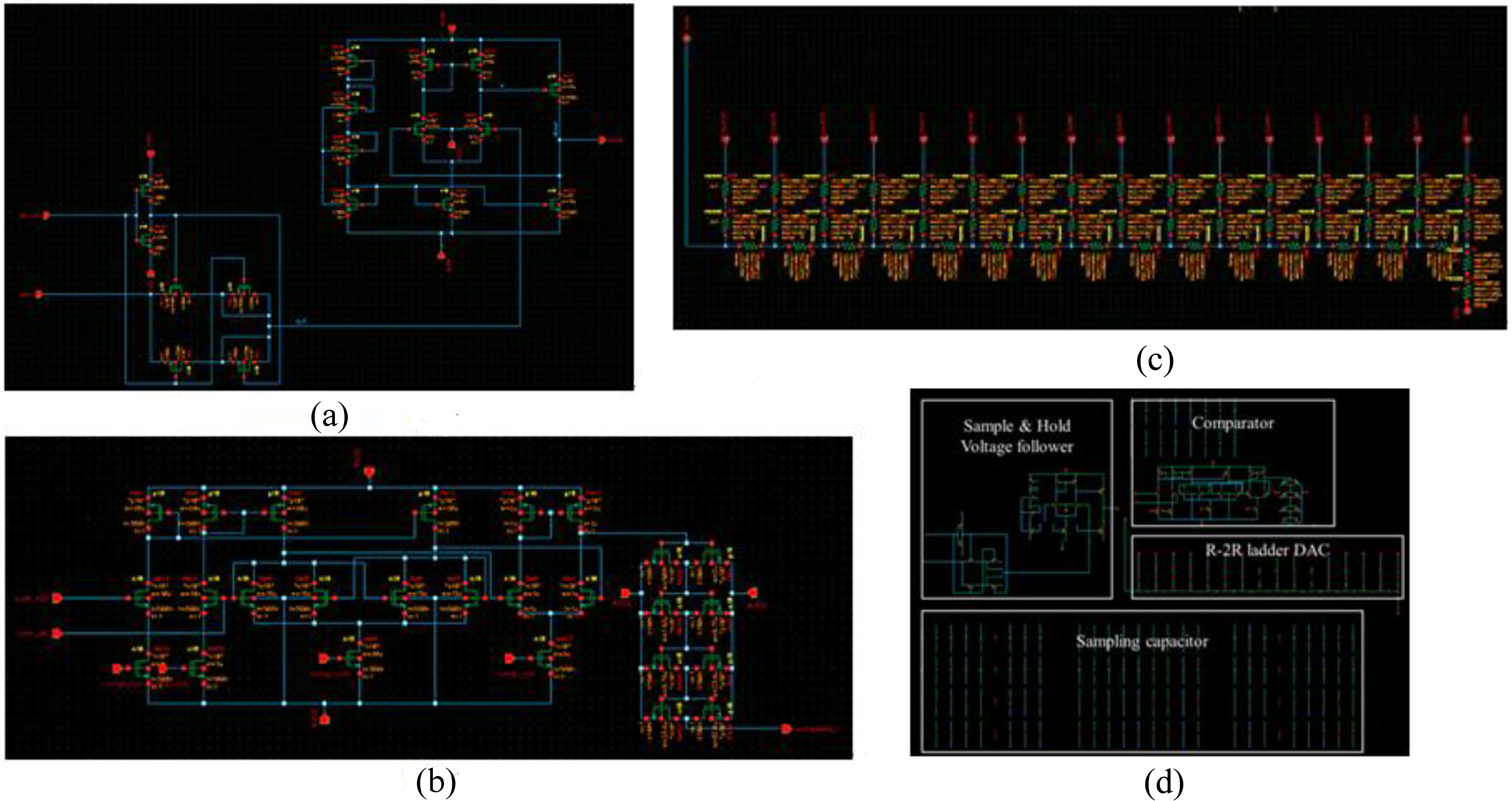
The designed SAR ADC consists of sample and hold, a voltage follower, comparator, and R-2R ladder DAC, as shown in Fig. 4. Therefore, the SAR ADC design focused on low power consumption and a small size.
Figure 4.
Entire circuit diagram of (a) sample and hold, (b) comparator, (c) R-2R ladder DAC, (d) designed SAR ADC.
The designed sample and hold circuit consists of switches, a sampling capacitor, inverter, and voltage follower. If the switch works in the on/off positions, the charge injection and clock feedthrough will be produced by a parasitic capacitor. This problem affects the linearity due to the leakage current. In order to solve the problem of non-linearity, there are ways to reduce the size of the switch and increase the value of the sampling capacitor. However, increasing the value of the sampling capacitor also increases the size and power consumption. In order to reduce the leakage current, the switch size is minimized. In addition, the charge injection is an element that disturbs linearity. In order to prevent the charge injection, a CMOS switch and dummy switch have been used. Because the electric charges of the NMOS and PMOS have opposite polarity, the charge injection is reduced. The non-linearity problem is compensated for by the preceding method, but not completely resolved. Therefore, bit conversion is performed before the occurrence of LSB error due to the non-linearity problem, as shown in Fig. 5. The LSB error is caused in about 7
Figure 5.
Entire circuit diagram of designed SAR ADC.
Figure 6.
Simulation results of (a) sample and hold, (b) R-2R ladder DAC comparator.
Figure 7.
The calculated average power consumption and current simulation of designed SAR DAC.
Figure 8.
Overall layout of designed SAR ADC.
In the SAR ADC, the comparator is a circuit that plays an important role in the ADC as a quantizer of 1 bit, and it produces a digital signal that compared with the output of the sample and hold and the DAC. The structure of the comparator consists of an amplifier, latch and buffer. In order to minimize the offset voltage and power consumption of the designed comparator, we designed a preamplifier with current mirror. Therefore, the power consumption was reduced by the power control switch used in the comparator. A stable output was obtained by the buffer.
2.3Simulation of designed SAR ADC
In this paper, we designed an SAR ADC for fully implantable hearing aids. The circuit simulation was performed using the Spectre circuit simulator (Cadence, USA). The simulation result of the designed SAR ADC is shown in Fig. 6. As a simulation result, the analog input signal was sampled and was held by a control signal. Thus, the R-2R DAC output has been approximated to the held signal input and we confirmed that the corresponding digital code was output. The current simulation was performed using a circuit simulator Spectre (Cadence, USA), as shown in Fig. 7. The average power consumption was calculated by Eq. (1), which was provided in the simulation software, where
(1)
3.Results
The layout of the designed SAR ADC was performed by Virtuoso Layout Editor (Cadence, USA), as shown in Fig. 8. In the layout result, the size of the designed SAR ADC occupied 124.9
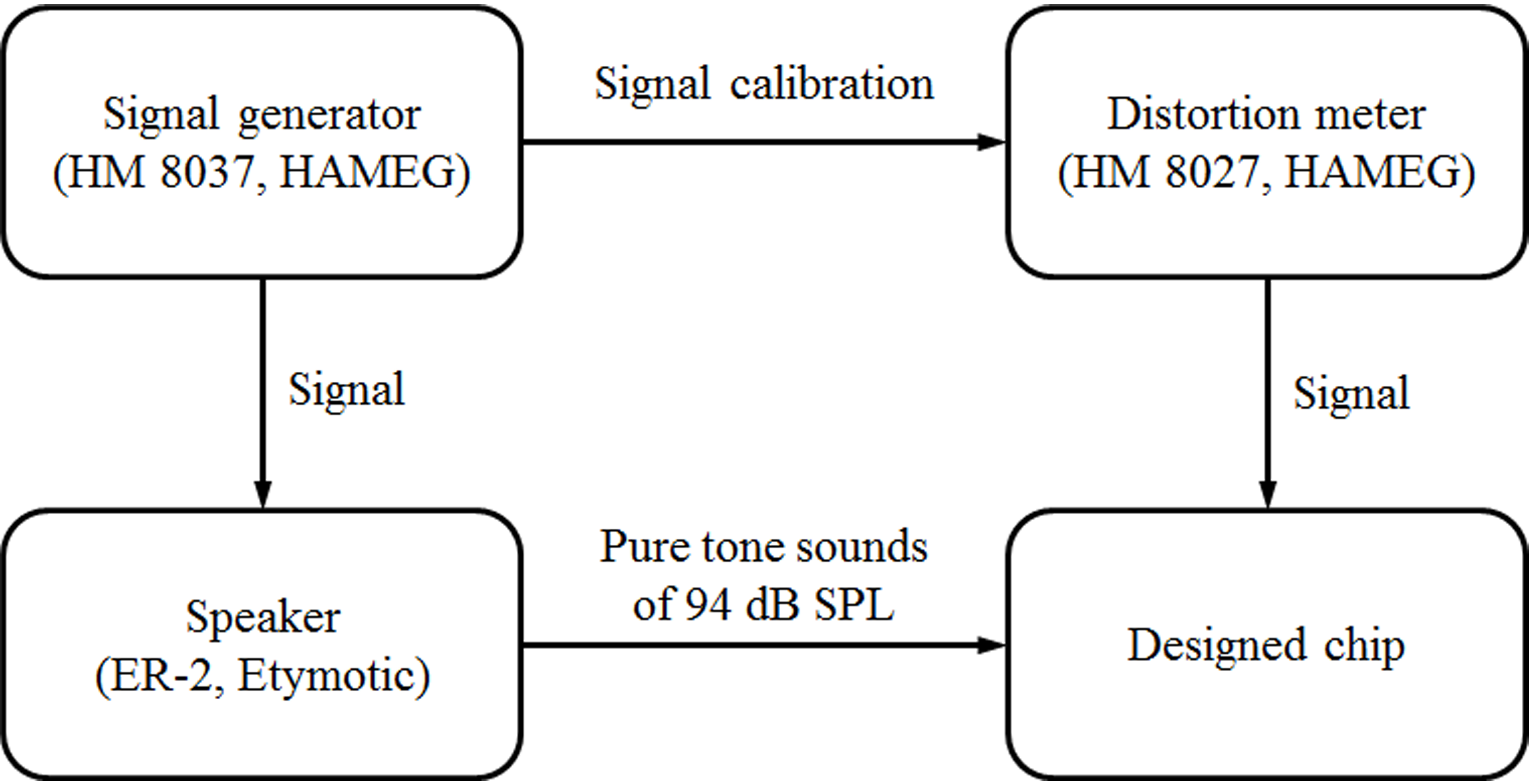
The total harmonic distortion (THD) of the fabricated chip was evaluated by the ANSI. s3. 22. 2003 standard. The experimental block-diagram for the THD evaluation is shown in Fig. 10. The SAR ADC output was measured using a distortion meter (HM 8027), when applying pure tone sounds of 94 dB SPL at 500, 800, and 1600 Hz regions. The results of the THD evaluation are shown in Table 3. As a result, the THD performance of the proposed chip was satisfied with the ANSI. s3. 22. 2003 standard.
Table 3
Performance table of manufactured SAR ADC
| 70dB SPL @ 500 Hz | 70dB SPL @ 800 Hz | 65dB SPL @ 1600 Hz | |
| THD | 1.5% | 1.7% | 1.3% |
Figure 9.
Operation waveform of the designed chip.
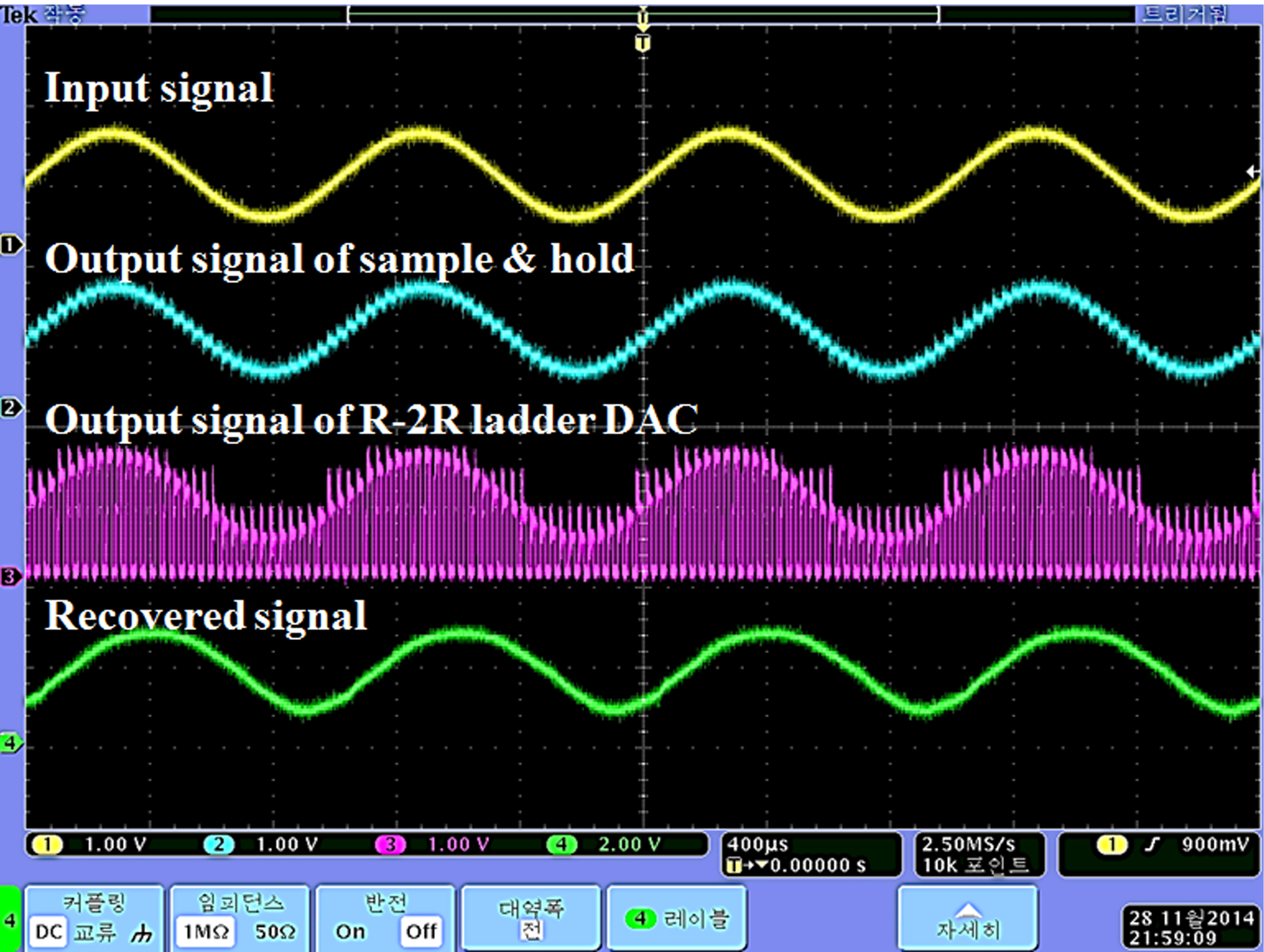
Table 4
Performance of manufactured SAR ADC
| Sigma-delta | SAR ADC | Manufactured SAR ADC | |
|---|---|---|---|
| Reference | Choi et al. (2007) | Frank et al. (2012) | |
| Supply voltage | 3 V | 1.2 V | 1.8 V |
| Resolution | 16-bit | 16-bit | 16-bit |
| Power | 5.6 mW | 1.5 mW | 50.04 |
| Size | 0.89 mm * 1.38 mm | 0.85 mm * 1.72 mm | 0.125 mm * 0.152 mm |
| process | 180 nm CMOS | 180 nm CMOS | 180 nm CMOS |
Figure 10.
Block diagram of experimental setup for measuring distortion of manufactured SAR ADC.
In this paper, the operation of the manufactured SAR ADC for fully implantable hearing aids was verified by using a MSO 4034 oscilloscope (Tektronix, USA) and computer simulation. The performance of the manufactured SAR ADC is shown in Table 4 [10, 11]. As a result, the manufactured SAR ADC had an advantage in power and area compared with the conventional ADC and was confirmed to meet the fully implantable hearing aid characteristics.
4.Conclusion
In this paper, we proposed a low-power 16-bit 32 kHz SAR ADC for fully implantable hearing aids. The power consumption is 50
Conflict of interest
None to report.
Acknowledgments
This work was supported by the National Research Foundation of Korea (NRF) and grant funded by the Korean Government (MSIP) (No. 2016R1A2A1A05005413 & No. 2015R1D1A1A01060439), and This research was financially supported by the Ministry of Trade, Industry and Energy (MOTIE) and Korea Institute for Advancement of Technology (KIAT), DaeGu Institute for Regional Program Evaluation (IRPE) through the Research and Development for Regional Industry (R0004188).
References
[1] | Kroll K, Grant IL, and Javel E, The Envoy totally implantable hearing system, St. Croix Medical, Trends in Amplification, (2002) ; 6: (2): 73-80. |
[2] | Kim HH, and Barrs DM, Hearing aids: a review of what’s new, Otolaryngology-Head and Neck Surgery, (2006) ; 134: (6): 1043-1050. |
[3] | Kim D, Senog K, Kim M, Chao J, and Lee J, A 1-Channel 3-Band Wide Dynamic Range Compression Chip for Vibration Transducer of Implantable Hearing Aids, Bio-medical Materials and Engineering, (2014) ; 24: (1): 1009-1017. |
[4] | Grilo J, MacRobbie E, Halim R, and Temes G, A 1.8 V 94 dB dynamic range ΣΔ modulator for voice applications, 1996 IEEE International Solid-State Circuits Conference, (1996) : 8-10. |
[5] | Yao L, Steyaert MSJ, and Sansen W, A 1V 140uW 88dB Audio Sigma-Delta Modulator in 90 nm CMOS, IEEE J. of Solid-State Circuits, (2004) ; 39: (11): 1809-1818. |
[6] | Fletcher H, Auditory patterns, Reviews of Modern Physics, (1940) ; 12: (1): 47. |
[7] | Puder H, Hearing aids: an overview of the state-of-the-art, challenges, and future trends of an interesting audio signal processing application, In: Proceedings of 6th International Symposium on Image and Signal Processing and Analysis, (2009) : 1-6. |
[8] | Lee KW, Lee JH, and Kim K, Hearing Aid Evaluation, Hakjisa, (2007) : 11-27. |
[9] | David AJ, and Ken M, Analog integrated circuit design, John Wiley& Sons, Inc, (1997) . |
[10] | Choi YK, Roh HD, Byun SH, Nam HS, and Roh JJ, Design of a 99 DR single-bit 4th-order High Performance Delta-Sigma Modulator, The institute of electronics and information engineers, (2007) ; 44: (2): 25-33. |
[11] | Ohnhaeuser F, and Bialek J, A 1.5 mW 1 MSPS 16 bit SAR ADC with high performance, Semiconductor Conference Dresden-Grenoble (ISCDG), 2012 International. IEEE, (2012) : 9-12. |