
A Novel Automated Interoperability Test and Debug System for Near-Field Communication
Abstract
In this article, we present a new system architecture of an automated interoperability test and debug system for Near-Field Communication (NFC). The increasing availability of NFC-enabled devices and the resulting amount of NFC applications require new methods for interoperability testing and debugging in order to reduce costs. We combine already existing interoperability test systems and the know-how of manual debugging methods to develop a new automated interoperability test and debug system architecture. We analyze the main components of state-of-the-art test systems, define new requirements for the new system architecture, and evaluated the feasibility with two different designs. Our new system architecture significantly reduces the time and cost of developing and certifying new NFC-enabled devices.
1Introduction
Near-Field Communication (NFC) is a wireless communication technology for convenient and secure data exchange over a short distance. Use cases can be found in a wide range of different applications like access control, payment, public transport, fare collection, ticketing, data sharing, smart poster, and many more (Finkenzeller, 2010; Lacmanović, Radulović, & Lacmanović, 2010; NFC Forum, 2007). All these different application types work well in their own ecosystems because of different standardization bodies defined and implemented their specific standards. For example, in ISO/IEC 14443, the 13.56MHz interface is defined for applications such as access control, fare collection, and ticketing. However, the EMVCo standard defines the same interface for payment application. The standard ISO/IEC 18092 again uses the same interface to define the so-called peer-to-peer mode, which allows communication between two NFC-enabled devices (Shobha, Aruna, Bhagyashree, & Sarita, 2016).
Due to the different requirements, standards, and implementations of the contactless interface, interoperability cannot be guaranteed. Although the NFC Forum has already harmonized some parts of the different standards, interoperability testing is still necessary. Extensive conformance testing is not enough to ensure interoperability between different NFC-enabled device from various manufactures (Kang, 1998).
Interoperability testing became an even more and more complicated topic due to the constantly increasing number of different NFC-enabled devices and the resulting number of NFC applications. To identify interoperability problems as early as possible numerous debug sessions should be included in the development process (Boada, 2016). CISC Semiconductor is a global player in RFID and NFC test equipment and offers interoperability testing as a service. The last years of supporting leading NFC-device manufactures showed that the most time consuming and therefore, most cost intensive task during interoperability testing, is manual debugging in case of a communication error (CISC Semiconductor, 2018). To find the root cause of a communication error, additional measurement equipment, a protocol analyzer, signal processing software and expert know-how about the protocols and the physical transport layer is required.
In this article, we present a new architecture of an automated interoperability test and debug system for NFC. By including analog measurement equipment, advanced signal processing, improved data visualization, and error classification algorithms, the following goals can be achieved:
• The integration of the analog measurement system into the automated test system avoids additional manual test runs in case of a communication error. Therefore, less debug sessions are necessary.
• During the development of a new NFC-enabled device, the error classification algorithm supports the engineer in finding the root cause of communication errors much faster. The new automated NFC interoperability tests and debug system thus reduces the development time for NFC-enabled devices.
• Due to the integration of additional equipment and new signal processing methods into the automated test system, less know-how about the NFC communication interface and the application-specific protocols is required. Thereby, the usability of the test system is increased, and it can be used by a larger number of people.
This article is organized as follows. Section 1 describes basic background information about the NFC technology and Section 2 presents the state-of-the-art NFC interoperability test system. Section 3 describes some related works, and Section 4 points out the new requirements and issues to the new automated interoperability test and debug system, which is then further described in Section 5. Section 6 is split up in four subsections, where the first two show the design and the results using the RedPitay platform. However, the remaining two describe the design and the results implemented on the LimeSDR platform. Section 7 finally concludes this article and describes some future work.
2Background
This section describes some background information about the NFC technology, which is essential for the new automated NFC interoperability test and debug system.
NFC was developed by NXP Semiconductors and Sony back in 2002. They combined ISO/IEC 14443 Type A (also known as MIFARE) with the Japanese industry standard JIS X 6319-4 (also known as FeliCa). NFC works up to a distance of 10cm, with a maximum data rate of 424kBit/s, at a frequency of 13.56MHz and is compatible to already existing RFID standards (Langer & Roland, 2010). NFC supports three different operating modes, peer-to-peer, read/write, and card emulation (Coskun, Ozdenizci, & Ok, 2015; Finkenzeller, 2010).
• The peer-to-peer mode allows two smartphones to exchange data such as contacts or credentials for Bluetooth or WiFi. The smartphone which starts the communication is termed the NFC-initiator and the other one the NFC-target. Both the NFC-initiator and the NFC-target use amplitude shift keying (ASK) modulation for communication.
• In read/write mode, one NFC-enabled device is the active device and provides the energy for the passive NFC tag. The active device, known as the reader/writer, uses ASK modulation. The passive NFC tag, however, uses load modulation. The reader/writer is able to read data from passive NFC tags such as NFC smart posters, payment cards to mention only a few. In case the NFC tag is not configured as read-only, an NFC writer can access the tag and write data to it.
• In card emulation mode, one NFC-enabled device acts like a passive NFC tag. The used modulation is the same as in read/write mode. The active NFC-enabled device uses ASK modulation, and the NFC-enabled device that supports the card emulation mode uses load modulation.
3State of the art
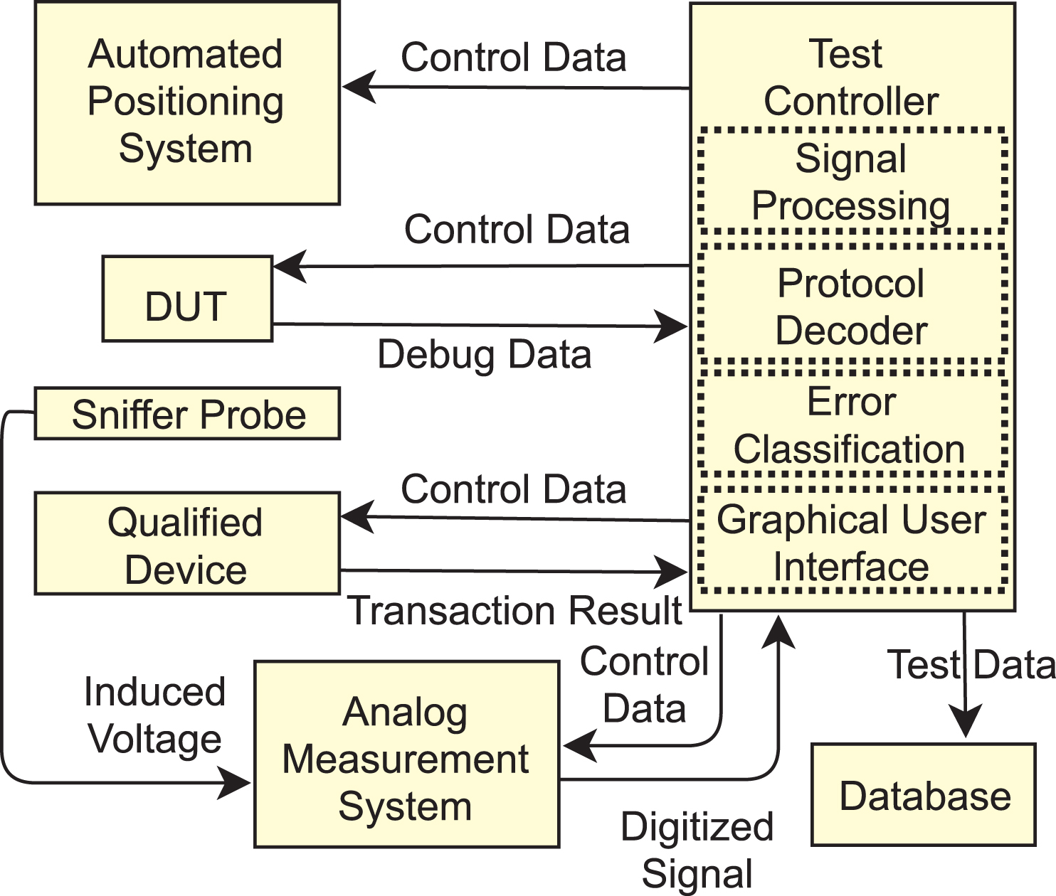
Fig. 1 points to the problem that even if the two communication partners are compliant to their standards, conformance testing does not replace interoperability testing. This issue is also well elaborated in the work of the Korean Telecom research and development group (Kang, 1998). It is true that conformance testing covers a huge amount of possible errors, but interoperability testing really ensures successful and reliable communication. Furthermore, conformance requirements are derived from the implemented standards, and therefore, user requirements may not be addressed perfectly. Existing test approaches (CISC Semiconductor, 2018; Comprion, 2019; Couraud, Vauche, Deleruyelle, & Kussener, 2015; FIME, 2019; Hawrylak, Ogirala, Cain, & Mickle, 2008; Langer, Saminger, & Grunberger, 2009; Micropross, 2018) share a common system architecture that is illustrated in Fig. 2. The implementation of each component may vary from different developers and researchers, but the main functionalities are more or less the same. This section describes the main components of a state-of-the-art NFC interoperability test system and points out the most important features.
Fig.1
Conformance and interoperability testing.
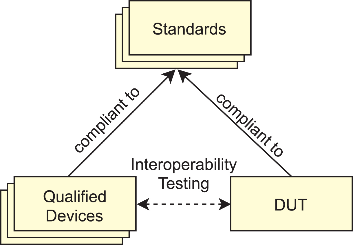
Fig.2
State-of-the-art NFC interoperability test system.
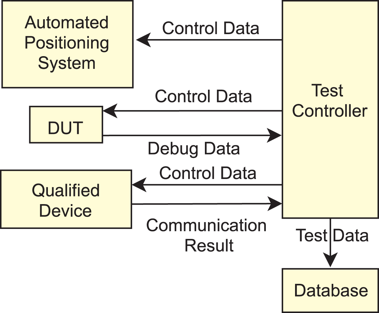
Qualified Device: In order to perform NFC interoperability tests, many already qualified devices are required. Qualified devices are the communication partner for any of the possible operating modes defined within the different standards and described in Section 1. They need to be compliant to their implemented standards, as shown in Fig. 1 and be already certified devices. These devices are used as a verified reference to test the devices under test (DUT). A larger amount of qualified devices used in a test leads to a much more meaningful test result.
If a qualified device acts as communication initiator, it needs to be controllable via an external interface. Such an interface is usually a USB or Ethernet connection and connects the qualified device with the test controller. Each qualified device has its own instruction set and therefore needs its own communication interface implementation on the test controller. Some qualified devices return additional debugging information, which subsequently can be helpful for error detection, but unfortunately, such debug interfaces are not accessible for qualified devices in most cases.
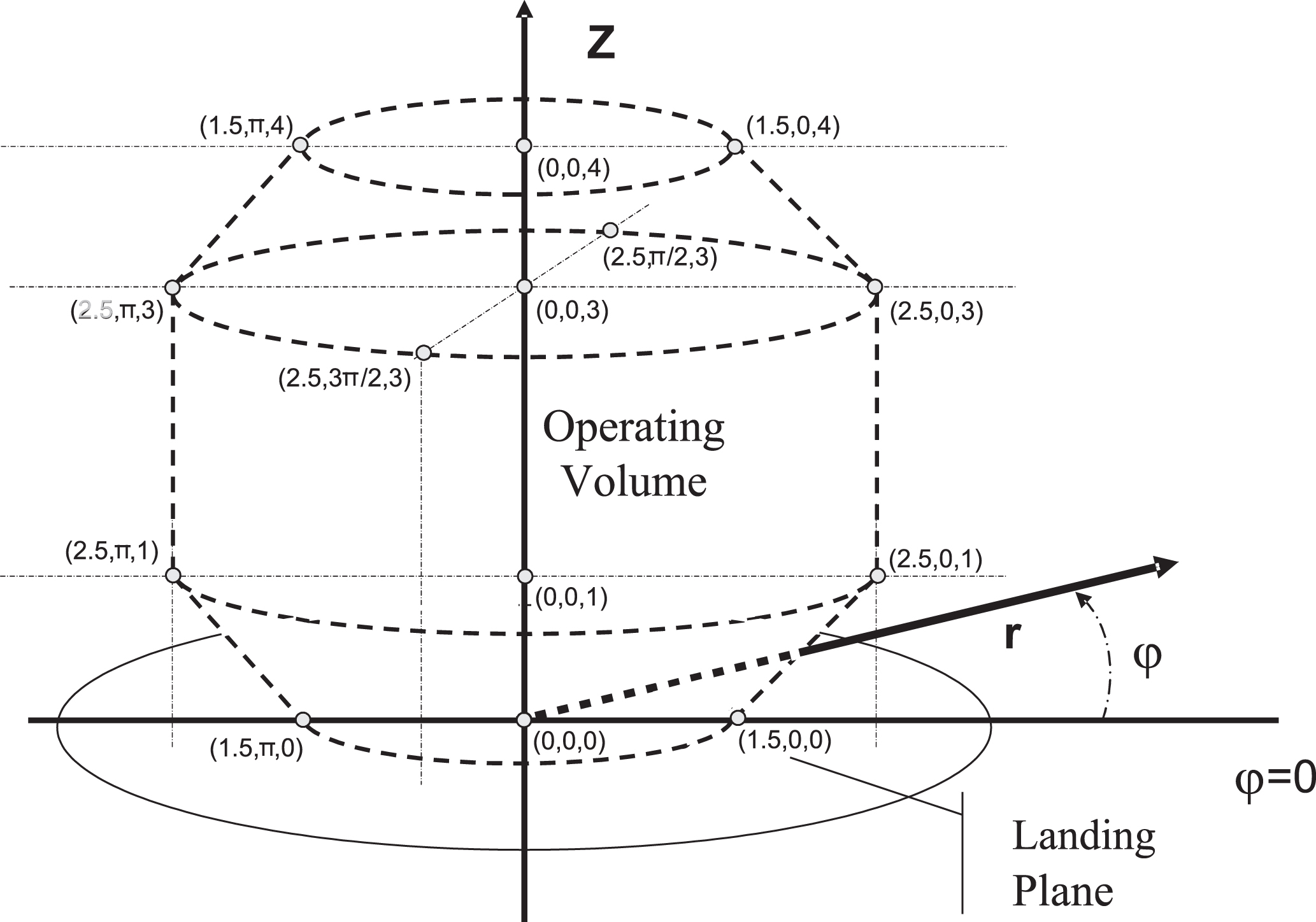
Automated Positioning System: There are many different approaches for an automated positioning system. Some of these work like a robot arm, others more like a 3D-printer. However, all of them need to fulfill the criteria given by the various standards. The most important criteria are a well-defined reference starting point, very accurate step motors, the possibility to move the DUT in three dimensions and controllable through an interface by the test controller (CISC Semiconductor, 2018; DENSO Robotics, 2019; FIME, 2019; Langer et al., 2009; Sun & Wang, 2014). Fig. 3 shows the operating volume for secure payment applications defined by the EMVCo standard (EMVCo, 2016). To test devices that implement this secure payment standard, the automated positioning system needs to be able to move the DUTs within this defined volume. Other applications define a different operating volume. Therefore, the automated position system is designed to cover many of the different defined operating volumes. Robots that provide the possibility to rotate the DUT and change its angle allow to simulate the user behavior even more precisely. The most important requirement is that the robot needs to guarantee that all measurements, during multiple test runs are performed at the very same positions. This also requires well-defined positions for the qualified devices among different test runs.
Fig.3
EMVCo operating volume (EMVCo, 2016).
Device Under Test: A DUT can be an already finished product or an evaluation board. Depending on the used qualified devices, the DUT can either be a PICC (proximity integrated circuit card) or a PCD (proximity coupling device). However, interoperability testing is essential during development, and therefore in most cases, an NFC evaluation board or a prototype is used. A very important advantage of using a non-finished product is an additional debug channel between DUT and test controller, which in most final products is not accessible anymore. In some cases, the DUT gives the possibility to change parameters vie software. Therefore, the test controller needs to implement this additional interface to control the DUT.
Database: A simple database is used to store test relevant information and keep test results organized among multiple test runs. The stored information is used, on the one hand, to generate test reports and, on the other hand, to reproduce test results as good as possible. Environment information such as temperature, humidity, and pressure are as important to store in the database as DUT information, qualified device information, timestamps, and measured volume positions with the corresponding communication results.
Test Controller: The test controller, can be implemented on a conventional PC as shown in (Couraud et al., 2015; Hawrylak et al., 2008; Langer et al., 2009) or on a more task-specific computer as shown in (Kun et al., 2009) and acts as the central unit of an NFC interoperability test system. The test controller implements all the interfaces needed to control, monitor, and evaluate the test behavior. One interface is needed to control the automated positioning system. The test controller needs to ensure the correct position of the DUT. It is also responsible for changing the position after or during a communication of those devices which require this feature to conclude the communication successfully. Qualified devices can provide an Ethernet or USB connection. To connect multiple qualified devices, Ethernet switches and USB-hubs are used. The test controller needs to provide these two interfaces to control and read back the communication results from each qualified device. In case the database is not implemented locally on the test controller, an additional interface is required to connect the database. As already mentioned, some DUTs such as development boards and prototypes may have additional control and debug interfaces for obtaining more detailed information about the performed communication. In these cases, the test controller needs to implement these additional interfaces to control the DUT and collect debug information.
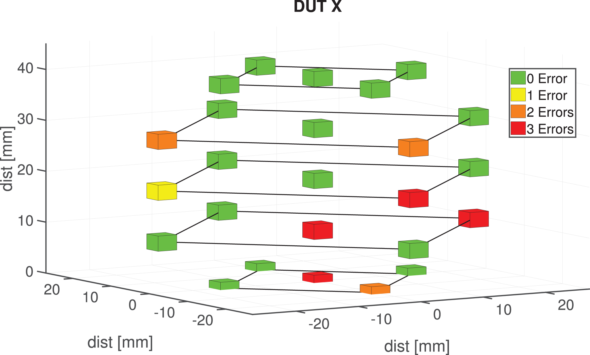
The result evaluation of a common test controller in most of the cases is straightforward and based on the communication result of the qualified device. The communication may either be successful or fail. In the latter case, only the additional interface to the DUT, if available, can deliver more precise information about the failure. A possible result is shown in Fig. 4. The green cubes show all measurement points with three out of three successful communications. At the positions marked with yellow cubes, two out of three communications were successful, whereas orange cubes represent one out of three successful communications. Positions with no successful communication within three tries are marked with red cubes. Such visualization is mostly not very helpful in the event of an error, and the automated test system has no further data for detailed error analysis. Additional manual debugging systems are thus needed, such as protocol analyzer and analog measurement equipment. An engineer will need to perform the required measurements again manually, analyze the measured data with additional software, and try to find the error. A qualified engineer, additional test-runs, additional measurement equipment, and additional debug time are thus required.
Fig.4
CISC Semiconductor test result (CISC Semiconductor, 2018).
4Related work
The NFC Forum cooperates with other standardization organizations such as ISO/IEC, EMVCo, GSMA, etc. to harmonize the different standards and to define new specifications. The goal of the standard harmonization work is to increase the interoperability among different NFC-enabled devices by defining detailed conformance tests and by supporting so called plugfests. Plugfests are events where developer can test their products against others to detect interoperability problems. At this point, it is not mandatory to participate such plugfests, and the certification will not be denied in case of interoperability problems (Tagawa Koichi, 2011). Nevertheless, the test specification defined by the NFC-Forum and ISO/IEC can be used for basic requirements for the new automated interoperability test and debug system, especially for the analog measurement system and the signal processing tasks.
Researchers from the Upper Austria University of Applied Science in Hagenberg present in their publication (Langer et al., 2009) an automated NFC measurement and test system. It consists of the components shown in Fig. 2, extended with measurement equipment such as oscilloscope, protocol analyzer, etc. This test system can measure the electromagnetic field, test the collision avoidance, test read/write operations on NFC tags, test the communication speed adaption, and analyze the used protocols. The implemented test cases are part of the NFC Forum test specification and the two standards ECMA-356 (ECMA, 2014b) and ECMA-362 (ECMA, 2005). The described test system can be used as an interoperability test system, but in case of communication errors, only failures related to the electromagnetic field or the protocol can be detected. In contrast to the new automated interoperability test and debug system for NFC described in this article, the test system described above focuses more on performance testing. Moreover, the electromagnetic field strength is only one of many NFC communication relevant parameters. However, the new automated NFC interoperability test and debug system combines the additional measurement equipment in one analog measurement system and shifts the complex data analysis tasks to the test controller.
In the work (Couraud et al., 2015), the researchers present a test platform for very high bit rate communication using ISO 14443. The primary purpose of the presented test system is to evaluate the signal quality of the PICC under test. Therefore, they developed an FPGA device to send specific commands, using the ISO 10373-6 test setup to the PICC and to record the response for further evaluation. They provide a possibility to use the proposed system to test interoperability. To do so, waveforms from different readers can be recorded and replayed whenever the given reader should be used to test interoperability. Using this technique comes along with a few drawbacks. The behavior of one single reader for different distances between the reader and PICC is not the same, so one would need to record many different measurement points for one reader. During recording such a waveform, a coil needs to be present in the H-field of the reader and, therefore, changes the behavior of the reader. These uncertainties are then forwarded to the following interoperability tests. Additionally, the PICC under test has another influence on the antenna of the test setup than under real conditions using a reader. To overcome this problems, the novel automated interoperability test and debug system for NFC introduced in this article uses one closed system where readers and DUT‘s are handled as a black box, and different behavior of the readers are generated by changing the distance using the automated positioning system. Nevertheless, FPGA design decisions can be used for the analog measurement system.
The automated interoperability test system at CISC Semiconductor fits very well the system described in Section 2 (CISC Semiconductor, 2018). They use a positioning robot to move a DUT within the EMVCo specified operating volume of different readers, a standard PC for test automation, and the Xplorer (CISC Semiconductor, 2019) for detailed communication analysis. The disadvantage of the automated interoperability measurement system at CISC Semiconductor is that the report generated automatically after a test run contains only the success rate of the transactions performed at the different positions. For detailed error root cause analysis, additional transactions at the error positions need to be performed manually. The signal traces captured with the Xplorer can than be used for further manual protocol and signal characteristic analysis. The new automated interoperability test and debug system for NFC, presented in this article, improves the automatically generated test outcome by providing more detailed information about the failure reason. Furthermore, the manual debugging process is automated. The test execution time and test costs are thus reduced. In contrast to the systems developed by the approaches mentioned above, the new automated NFC interoperability test and debug system is designed to be used by people without any in-depth knowledge of NFC protocols.
5Requirements and issues
As described in Section 3, companies, and researchers put effort in developing new measurement systems for specific parameters or in automating the test procedure to improve the test results, save overall test time and reduce the associated costs. None of the available solutions provide enough information in the case of a communication error, is fully automated, and can be used for interoperability testing. The new automated NFC interoperability test and debug system tackles exactly these problems by defining new requirements and proposing solutions for additional upcoming issues.
Reduce Manual Debugging Time: One of the most important requirements for the new automated NFC interoperability test and debug system is reducing the time an engineer needs to spend evaluating test results and searching for communication error root causes. In order to fulfill this requirement, the architecture of the new automated NFC interoperability test system must include solutions to automate time-consuming tasks that are currently performed manually by an engineer.
Analog Measurement System: A communication error can occur either on the protocol layer or on the physical transport layer (ECMA, 2014a; National Instruments, 2013). To detect both types of communication failures, the electromagnetic field between the two communicating devices needs to be captured. To measure the electromagnetic field, an additional coil, called sniffer probe, is placed between the two NFC-enabled devices. The induced voltage of the sniffer probe is measured by a suitable analog-digital converter (ADC). Test standards and test specifications define test methods and test equipment for certification authorities to ensure that every new certified NFC-enabled device has been tested under the same conditions. These standards can be used to derive the hardware requirements for the analog measurement system. In addition to the requirements extracted from the standards, the works in (Couraud et al., 2015; Hawrylak et al., 2008; Kun et al., 2009; Langer et al., 2009) provide possible solutions on how such requirements can be implemented. Important hardware requirements are sampling rate, RF bandwidth, ADC resolution, and ADC noise. Furthermore, the analog measurement system must be able to perform signal processing tasks for real-time signal preprocessing.
The high sampling rate requires a very high data throughput of the interface connecting the analog measurement system and the test controller. The data rate should thus be configurable in cases where less accurate measurements are sufficient. An additional trigger feature will simplify the capturing of the communication signal of interest and reduce the data, which needs to be transferred to the test controller. In addition to the data transfer interface, a USB connection shall be provided as a bi-directional communication channel between the test controller and the analog measurement system. This additional communication gives the test controller the possibility to send configuration commands and read back the state of the analog measurement system.
Automated Signal Analysis: This essential requirement for our automated interoperability test and debug system is responsible for reducing the manual debugging time. The automated signal analysis module will use the analog measurement system’s captured signal and compute communication relevant parameters. The signal processing or the parameter calculation may vary between the different operation modes described in Section 1. Parameters such as envelope timing, phase drift, modulation index are straightforward to calculate automatically. However, some other parameters require a very special selection of the captured communication signal, which is the complex part of the automated signal analysis. The new architecture of the automated interoperability test and debug system must also automatically perform the more complex parameter calculation. The more communication relevant parameters can be calculated, the more different error cases, it will be possible to analyze automatically.
Protocol Decoder: To guarantee interoperability a proper protocol implementation is essential. During debug sessions, it is beneficial to know if communication errors occur on PCD or PICC side. Therefore, companies and research teams implement protocol analysis features in their test systems (CISC Semiconductor, 2019; Comprion, 2019; ECMA, 2005; Hawrylak et al., 2008; Kun et al., 2009; Micropross, 2018). Such a protocol decoder shall be included in the new architecture and decode the captured signal from the analog measurement system. One important feature of the protocol decoder is to detect errors and classify them automatically to reduce the required protocol know-how of the test engineer.
Error Classification: The automation of signal processing, parameter calculation, and protocol decoding gives the possibility to use all the extracted communication information to implement an error classification algorithm. An algorithm will indicate the communication error type and support the engineer in finding the actual error root cause.
Database: Because the captured signal traces are part of the test result evaluation; they should be stored and organized in such a manner that the link between test run and captured signal traces is not lost. A database infrastructure shall tackle this problem and guarantee data integrity. Therefore, the database of the new automated interoperability test and debug system shall store the captured signal traces together with the already stored test relevant information. Besides, the calculated communication relevant parameters shall also be stored. The database hardware, the software used, and the communication interface to the test controller shall be able to handle the larger files and higher amount of data compared to a state-of-the-art automated NFC interoperability test system.
Graphical User Interface: The new automated NFC interoperability test and debug system shall provide an easy to use and well organized graphical user interface. In addition to the hardware and communication configuration options, the visualization of the different measured signal traces and computed parameters will support the engineer in the task of rapidly evaluating the test results.
6Novel hardware and software architecture
Fig. 5 shows the improved architecture compared to the NFC interoperability test and debug system as shown in Fig. 2. This section describes the improvements of the new automated NFC interoperability test system, which meets the requirements and solves the issues described in Section 4. The necessary hardware changes are described in the following Section 5.1. The new software architecture, however, is described in Section 5.2.
Fig.5
New automated interoperability test and debug system architecture.
6.1Hardware architecture
The most complicated part regarding the new hardware architecture is the analog measurement system, which is used to capture the communication between two NFC-enabled devices. In order to measure the electromagnetic field as accurately as possible, three sniffer probes positioned, as shown in Fig. 6 are used. Sniffer probe 1 is used to capture the radiation of the electromagnetic field near the DUT, while sniffer probe 2 captures the radiation near the qualified device. Sniffer probe 3 is used to capture the electromagnetic field outside the operating volume to detect possible interferences to the test environment. The analog measurement system provides a Radio Frequency (RF) front-end to connect the three sniffer probes, an ADC to digitize the induces voltage, and a field programmable gate array (FPGA) for signal preprocessing. Due to the required sample rate of at least 500MS/s, which is required to calculate some communication relevant parameters, an FPGA mainboard with an additional analog measurement daughter board is used.
Fig.6
Analog measurement setup.
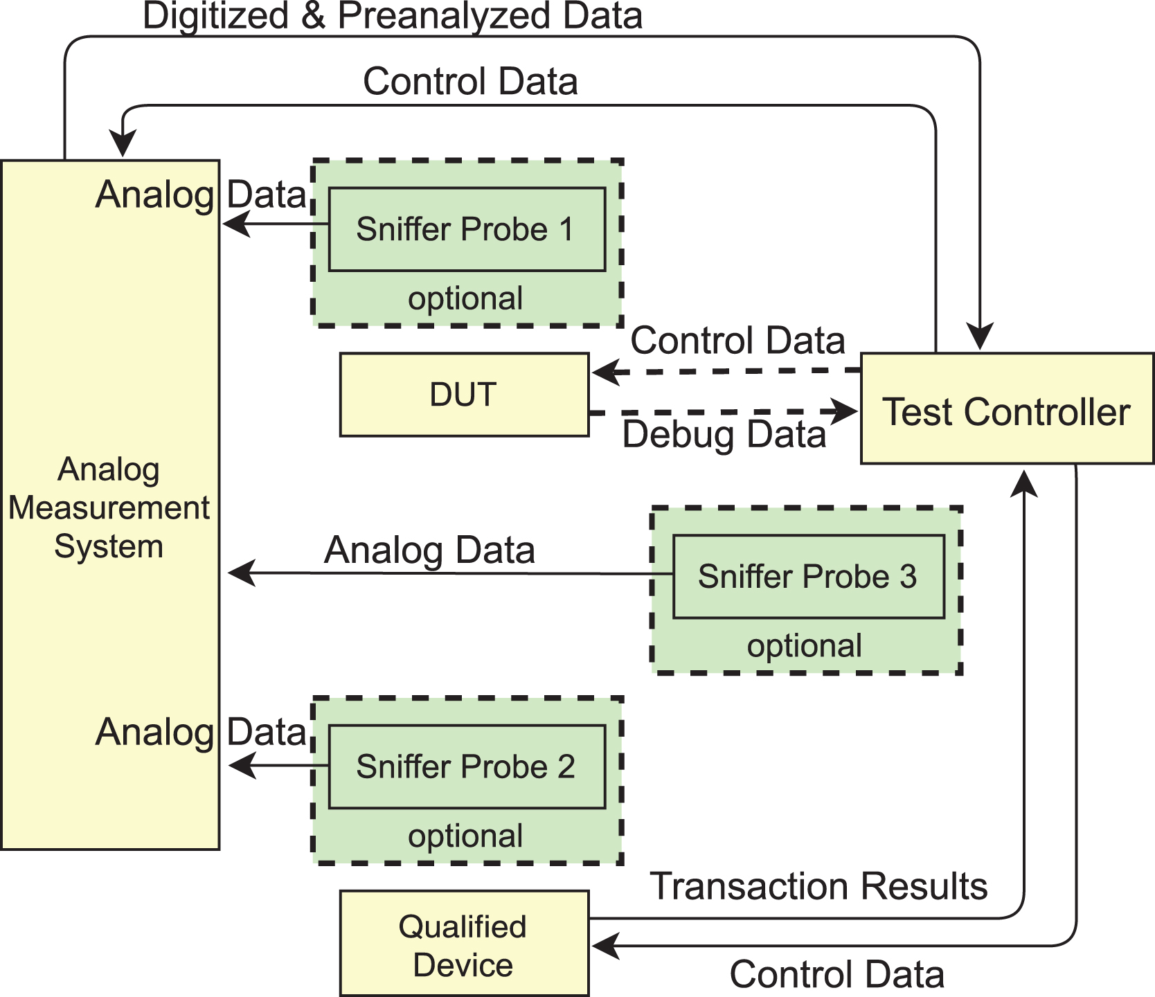
As automated positioning system we propose taking the best fitting described in Section 2. Only the three sniffer probes need to be mounted on the moving part of the positioning system. To compare the test results from multiple test runs, the sniffer probes’ position must always be the same.
The best platform to implement the test controller is a conventional PC because it is the best option to interconnect the different hardware interfaces and provides enough computational power to solve the signal processing tasks. The test controller of the new automated NFC interoperability test and debug system presented in this article is implemented on a modern PC. Another reason for implementing the test controller on a PC is the potentially required PCI interface for the analog measurement system.
6.2Software architecture
The new automated interoperability test and debug system for NFC requires a new extended software architecture to perform the required tasks described in Section 4. Three software components need to be implemented or extended. One concerns the test controller, the second one the analog measurement system, and the last one concerns the database.
The new test controller implementation is still responsible for controlling the qualified devices, the automated positioning system, the DUT, and the connection to the database. In addition to this, the new test controller needs to control the analog measurement system and overtake complex signal analysis tasks. On the one hand, a USB connection is used to control the analog measurement system. On the other hand, an additional interface (e.g., Ethernet, USB) is used to transfer the captured data to the test controller. After receiving the captured analog data, the communication result from the qualified device, and the optional debug data from the DUT, the test controller performs the result evaluation. Fig. 5 shows the four main tasks (signal processing, protocol decoding, error classification, and the graphical user interface) which are performed to analyze and display an NFC communication.
Signal Processing: Some signal preprocessing tasks are performed immediately by the analog measurement system. However, many further signal processing tasks are required to calculate the communication relevant parameters defined by the different test standards (e.g., ISO/IEC 10373-6 (ISO/IEC, 2016)). The test standards define upper and lower limits of different parameters and propose tools and algorithms to calculate them. The computed communication relevant parameter values are used as input for the error classification module. All these signal processing tasks are implemented in an automated manner and executed immediately if a communication error occurs. This fulfills the requirement of automated signal processing defined in Section 4. Furthermore, the signal processing software prepares the captured analog traces for the graphical user interface. This is important if an engineer wants to understand and analyze the captured communication in more detail.
Protocol Decoder: The protocol decoder takes the preprocessed communication signal from the signal processing module as input and tries to decode it. Since communication errors can occur on the protocol level, the result of the protocol decoder is necessary for successful error detection.
Error Classification: The main task of the error classification module is to assign the errors that have been occurred to a predefined class of errors and by this means to support the engineer in finding the root cause of communication errors. The error classification module implements a neuronal network to solve the classification problem. The calculated communication parameters from the signal processing module, the results from the protocol decoder, and additional information about the DUT are used as input for the neuronal network.
Graphical User Interface: For simple NFC interoperability test systems, a simple user interface for controlling the test runs and generating the test report is shown in Fig. 4 is sufficient. However, for the new automated interoperability test and debug system, the graphical user interface is improved. It displays the results from the protocol decoder, the captured communication traces from the analog measurement system, the results from the error classification module, and many more test relevant information. Furthermore, a more complex control view allows the setting of parameters for the analog measurement system and to control the test behavior. Parameters for the analog measurement system are, for example, the trigger level, the sampling rate, and the number of connected sniffer probes. The intuitive and user-friendly graphical user interface is crucial to speed up the debug process in case of a communication error.
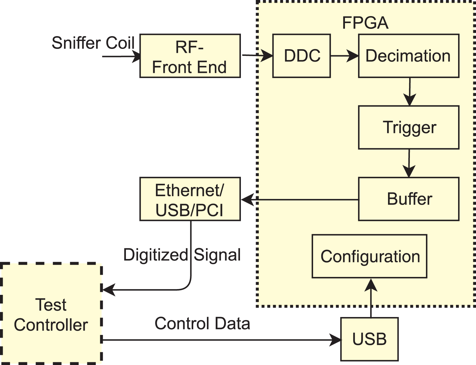
The second software part of the new automated NFC interoperability test and debug system is implemented on the analog measurement system. As described in Section 5.1, the analog measurement system consists of an FPGA that overtakes the real-time signal preprocessing tasks and is responsible for streaming the captured data over the selected output interface. The block diagram in Fig. 7 shows the main components of the analog measurement system. The configuration interface provides a set of commands to control the analog measurement system and to change the parameter of the different components. Such parameters are the trigger channel, trigger level, sample decimation rate, digital down converter (DDC) settings, enable/disable input channels, and select the output interface. The latter setting is required due to the possible high data rate, which exceeds the maximum data throughput of the Ethernet connection. If the decimation factor is high enough, or only one input channel is enabled, the sampled data can be transferred via Ethernet or USB to the test controller. The data rate can exceed the maximum Ethernet or USB communication speed. However, if the sample rate is too high and all channels are active. In this case, the faster peripheral component interconnect (PCI) bus can be used.
Fig.7
Overview of the Analog Measurement System.
The third software component of the new automated interoperability test and debug system concerns the database. It needs to handle the additional data collected by the analog measurement system during each test run. The architecture of the database fulfills the requirements described in Section 4. All the stored information about the different test runs can be used to generate test reports, compare the test runs, and reanalyze the results whenever needed.
By introducing all the new features described in this section, the manual debugging time is reduced. However, the overall test execution time increases slightly because of the additional tasks which have to be performed for every test point. Therefore, it is essential that the combination of different software, which is needed to implement the new tasks, is coordinated and synchronized perfectly.
7Evaluation
We first evaluated the feasibility of the proposed novel automated NFC interoperability test and debug system design with a proof of concept and then, as a second task, started developing the final hardware for the productive test system. The goal was to develop a low-cost proof of concept which meets the requirements described in Section 4 and implements the most important hardware and software features proposed in Section 5. The two designs are described in this section.
7.1Design RedPitaya
To evaluate the hardware requirements first, we chose the RedPitaya (StemLabs, 2018) platform to develop the analog measurement system. It provides two HF-inputs with a bandwidth of 50MHz, an ADC resolution of 14Bit, a sample rate of 125MS/s and a 1GBit Ethernet interface to transfer the data to the host PC. Additionally, the RedPitaya contains a Xilinx Zync 7010 system on chip FPGA with integrated ARM cortex-A9 and therefore meets our requirements very well. A sample rate of 500MS/s would be required for exact communication parameter measurement, but the main focus of our first proof of concept was to analyze the protocol layer. The ADC sample rate of 125MS/s is thus sufficient and reduces the complexity of the overall system. To further reduce the FPGA software complexity, we used only one HF-input to connect a sniffer coil, and the influence of the sniffer coil on the communication is neglected.
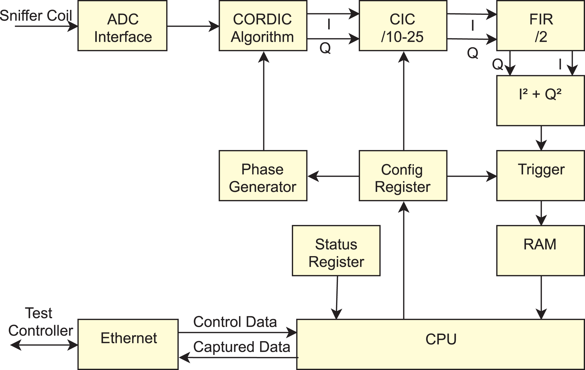
As described in Section 5, the FPGA is responsible for the real-time critical signal processing tasks. To evaluate this behavior, we implemented the signal processing chain shown in Fig. 8. However, Fig. 6 gives an overview of the proposed analog measurement system. Comparing these two figures, the only difference one can see is the Ethernet interface, which in our advanced version is used to transfer the captured samples to the test controller and to send control commands from the test controller to the analog measurement system. The signal preprocessing chain realized on the FPGA of the RedPitaya works as follows. We implemented a parameterizable phase generator and the CORDIC algorithm to obtain an IQ-data stream out of the ADC interface. The subsequent two filters are responsible to filter out the carrier signal and to reduce the sample rate. The first filter is a Cascade-Integrate-Comb (CIC) filter and reduces the sample rate by a configurable factor between 10 - 25. The second filter is a finite impulse response filter (FIR), which reduces the sample rate by factor two and filters with the cut-off frequency of 1.1MHz. The trigger functionality is responsible for detecting a rising edge of the signal overshooting the preconfigured value. Once the trigger detects such an edge, the following samples are stored to the random access memory (RAM) of the RedPitaya, and the appropriated status register is set. Subsequently, the samples are streamed to the test controller.
Fig.8
Implementation details of RedPitaya FPGA.
To evaluate the defined software requirements for the test controller described in Section 4 using the proposed designs from Section 5.2, we enhanced an already existing test controller. First, we implemented the Ethernet communication interface to transfer settings such as trigger level, the nominal carrier frequency for the phase generator, and the decimation value for the CIC filter to the RedPitaya. This interface is also used to start and stop capturing the analog signal received from the sniffer coil. The second implementation task was to transfer the captured data from the RedPitaya to the test controller and store it in the database. Furthermore, the test controller had to be extended by a protocol decoder to detect errors on the protocol layer. Finally, the graphical user interface, shown in Fig. 9 was added to the test controller to visualize the decoded protocol and the processed analog signal. The graphical user interface is designed in such a manner that it can also be used standalone combined with the RedPitaya as a manual debug tool to improve usability.
Fig.9
RedPitaya control and evaluation software.
7.2Results RedPitaya
After the successful development of the analog measurement device and the integration to the already existing NFC interoperability test system, we tested the complete system under real conditions. We mounted the RedPitaya on the moving part of the automated positioning system and fixed the sniffer coil on the DUT antenna. The automated positioning system moved the DUT with the mounted sniffer coil according to the volume shown in Fig. 3 over a selected payment terminal. The test controller stored all the test relevant data, including the analog signal traces from the analog measurement system to the database, and generated a report as shown in Fig 4. Fig. 9 shows one captured trace out of the whole test run. An engineer could now use the graphical user interface for further analysis.
The feasibility evaluation of the new system architecture using the RedPitaya design with the current implementation was successful, and no big issues in the system architecture were found. However, the RedPitaya platform and the current implementation is not the best solution to be integrated into a productive automated NFC interoperability test and debug system due to the following reasons.
Analog Frontend: The analog input frontend of the RedPitaya is very simple. With a jumper for each HF-input, the full input scale can be changed between ±1V and ±20V but there is no controllable amplifier. The induced voltage to the sniffer coil, which should be measured by the RedPitaya, depends on the shape and the number windings of the sniffer coil but also the distance to the signal source and the overall signal strength. The full scale of the ADC is thus used in only sporadic cases during a test run, which means the full 14Bit of the ADC are not used.
FPGA Utilization: Using the FPGA implementation shown in Fig. 8 the utilization of the different FPGA resources is around 20%, except the digital signal processing (DSP) units usage is already around 50%. Due to the sample rate of 125MS/s another approach has to be used instead of the required 500MS/s to calculate communication relevant parameters. The calculation of communication relevant parameters requires only one command and the corresponding response of a whole NFC-communication. Therefore, it would be possible that the RedPitaya will look for a command during the capturing process of the communication and trigger an additional external oscilloscope, which captures the command and the response with a higher sample rate. To implement this feature for the FPGA, numerous signal processing tasks would have to be taken on and solved, which according to our estimations, would no longer fit.
Test Controller Extension: The test controller extension with the graphical user interface to control the RedPitaya and to visualize the signal traces as well as the protocol decoder is directly implemented in Java. The reason for using Java was the more straightforward integration to the existing test system, but this also brings some severe shortcomings. Loading the captured signal traces and the protocol decoding, for example, already takes too long to be user friendly. The trace view of the graphical user interface provides no timing measurement features, which are very useful to analyze the analog signal shape and reacts slowly even if the trace is only about 100ms long. Furthermore, significant changes of the mean value for the overall signal trace need a manual change of the protocol decoder threshold to decode the signal trace without errors. In addition to the threshold problem, the protocol decoder is very unstable for noisy signals, because Java is not the best programming language to implement additional signal processing tasks.
7.3Design LimeSDR
Due to the limitations and problems with the RedPitaya platform, we decided to look for an additional different hardware platform, which solves the issues and meets the requirements described in Section 4 but is still a low-cost solution. After a research and evaluation period, we decided to go for a software-defined radio (SDR) approach using the USB version of the LimeSDR from Lime Microsystems (Myriad RF, 2019).
Lime Microsystems was founded in 2005 and, in the following years, developed the world’s first multiband LTE transceiver and the open-source strategy Myriad RF. Besides, various platforms were launched in cooperation with partner companies. Lime Microsystems specializes in field programmable RF transceivers (FPRF), SDR platforms, and ecosystem technology for the next generation of wireless broadband systems. These products offer an unprecedented level of configurability, enabling system designers to develop wireless communications network devices that can be tuned and reconfigured to run on any frequency for wireless communications and any mobile standard.
The LimeSDR provides six RF inputs for a continuous frequency range of 100kHz up to 3.8GHz and four RF outputs that can be used in 2x2 multiple-input multiple-output (MIMO) mode. The ADC has a resolution of 12Bit at a sample rate of 120MHz/s. A USB 3.0 interface is used to configure the LimeSDR and stream the data between the SDR and the host PC. The Altera Cycle IV FPGA and the dedicated FPRF transceiver, developed by Lime Microsystems make this hardware platform extremely powerful.
The FPRF transceiver implements a powerful analog frontend shown in Fig. 10 with different amplifiers, an analog mixer, and a configurable low-pass filter. This analog input stage is needed to shift the input signal to the baseband or to an intermediate frequency in case of very high input signal frequencies. After this first stage, the in-phase and quadrature (IQ) signal is sampled separately by the ADC and passed to the digital signal processing unit of the FPRF shown in Fig. 11. Three correction blocks for IQ-gain, IQ-phase, and direct current are implemented before the digital mixing stage. A decimation block and three general-purpose FIR filters complete the digital receiver path of the FPRF transceiver.

The powerful FPRF enables the possibility to shift the input signal to the baseband and apply all the required filters without using the FPGA, therefore saving its resources. Nevertheless, the sample rate of the LimeSDR does not reach the required 500MS/s. The FPGA is still unused, however, and the opportunity is thus given for using it to implement an intelligent command recognition feature. Such a feature allows detecting a specific NFC command in real-time and toggling one of the digital output pins of the LimeSDR. An additional oscilloscope connected to the sniffer coil and the digital output pin of the LimeSDR can be used to capture precisely one single command with the corresponding response. The time for an NFC command and response is that short, that the sample rate of the oscilloscope can be increased even further than 500MS/s. To enable this feature, the test controller needs to overtake additional tasks to control the oscilloscope. Such tasks are to ensure that the correct configuration is loaded to the oscilloscope and to arm the single shot trigger at the correct time and store the data once the oscilloscope captures the signal.
The entire controlling and analyzing software was reimplemented in MATLAB for two reasons. First, the performance of the Java implementation for controlling the RedPitaya and analyzing the protocol is very low. Second, the connection interface between the analog measurement device and the test controller changed from Ethernet on the RedPitaya to USB 3.0 on the LimeSDR. This increased the possible data throughput and the data volume to process on the test controller.
7.4Results LimeSDR
The integration of the control and analysis software for the LimeSDR implemented in MATLAB to the existing automated NFC interoperability test system was a much more difficult task, because the test environment is implemented in Java. Nevertheless, the advantages brought by MATLAB usage instead of Java for the signal processing tasks and the protocol decoder are numerous. The signal processing possibilities provided by MATLAB increase the success rate and the protocol decoder’s functional scope enormously. Additionally, the signal to noise ratio and the signal strength of the data processed by MATLAB can be much weaker compared to the Java implementation. However, the protocol decoder’s speed decreased slightly because of the much more sophisticated signal processing steps.
The issue that neither the RedPitaya nor the LimeSDR provides the sample rate required by the test standard can not be solved directly. Nevertheless, due to the FPRF on the LimeSDR, the FPGA provides enough free resources to implement a command detection feature and trigger an external oscilloscope. The MATLAB implementation can then be extended and analyze the command-response pair captured by the oscilloscope. Two drawbacks arise when using this approach— first, the need for an additional oscilloscope and the interface implementation to control it. Second, the additional effort to implement the command detection feature on the FPGA, but this is, in any case, a feature that would make the system more user friendly.
The additional FPRF transceiver on the LimeSDR saves very significant resources on the FPGA, but the more important advantage this brings is the powerful and configurable frontend. A frontend of this kind allows the user to shift the signal to the frequency needed and perform signal processing tasks before it is digitized. For our use case, the analog mixer is not so important because an input signal with a frequency of 13.56MHz can directly be sampled correctly with 120MS/s. The significant advantage in our case is the configurable amplifier stage, which allows us to amplify the input signal to the full scale of the ADC. Therefore, it uses the full 12Bit resolution.
8Conclusion
In this article, we present a new automated NFC interoperability test and debug system based on existing state-of-the-art interoperability test systems. Therefore, we define new hardware and software requirements and elaborate solutions for additional issues we came up with. The automated signal processing, signal analysis, and error classification we propose in this article reduce the manual debug time significantly. The decreased manual debugging time and the automatically calculated communication relevant parameter support the engineer during development and reduce the development time as well as the external certification duration.
The evaluation of the prototype we have developed so far shows that the main principles are feasible. The possibility to automatically capture the communication between two NFC-enabled devices and reanalyze the data stored in the database whenever needed increases the usability of the overall test system. To analyze specific NFC communication parameters, an external oscilloscope, or the development of a much more powerful analog measurement is required. The solution we provide with the LimeSDR and the external oscilloscope allows going for two different solutions. One is the low-cost variant, including simple parameter calculation and the protocol decoder. The second one makes use of the external oscilloscope, which is both more powerful and increases the information of the test output, but has the drawback of being more expensive.
Within the framework of the ANITAS project, we have implemented the low-cost variant and start to integrate it into our automated NFC interoperability test system. After the testing phase and further result evaluation, we will enhance the system and integrate the external oscilloscope, including the improved signal processing features.
Besides the development of the new automated NFC interoperability test and debug system, research regarding two important topics is ongoing. First, we will research on how different NFC controller settings influence the interoperability between NFC-enabled devices. A second topic is the influence of the used sniffer probes on the NFC communication, which we discovered out can be very significant.
Acknowledgments
This work is part of the ANITAS (Österreichische Forschungsförderungsgesellschaft, 2019) project in cooperation with CISC Semiconductor and NXP Semiconductors. This project is partly founded by the Kärntner Wirtschafts-förderungsfonds and the Steirischen Wirtschaftsförderungssgesellschaft mbH under the FFG grant number 864323.
References
1 | Boada, L. ((2016) ). Near Field Communication devices: having interoperability issues. Retrieved from https://blog.applus.com/ nfc - devices - having - interoperability-issues/. |
2 | CISC Semiconductor. ((2018) ). CISC Semiconductor Interoperability Website. Retrieved from https://www.cisc.at/services/nfc-interoperability-tests/ |
3 | CISC Semiconductor. ((2019) ). CISC Semiconductor Xplorer. Retrieved from https://www.cisc.at/products/nfc-xplorer/ |
4 | Comprion. ((2019) ). Comprion Website. Retrieved from https://www.comprion.com/products- solutions/products- solutions- a- z/emvco- l1- contactlesstest-solutions/. |
5 | Coskun, V. , Ozdenizci, B. , & Ok, K. ((2015) ). The Survey on Near Field Communication. Sensors, 15: (6), 13348–13405. doi: 10.3390/s150613348 |
6 | Couraud, B. , Vauche, R. , Deleruyelle, T. , & Kussener, E. ((2015) ). A very high bit rate test platform for ISO 14443 and interoperability tests. In 2015 IEEE 16th International Conference on Communication Technology (pp. 353–356). doi: 10.1109/ICCT.2015.7399857 |
7 | DENSO Robotics. ((2019) ). DENSO Robotics Product Overview. Retrieved from https://www.densorobotics-europe.com/_leadmin/Products/DENSO_Robotics_Product_Overview_EN.pdf |
8 | ECMA. ((2005) ). ECMA-362 NFCIP-1 - Protocol Test Methods. Retrieved from http://www.ecma-international.org |
9 | ECMA. (2014a). ECMA-340 NFCIP-1 - Near Field Communication – Interface and Protocol. Retrieved from http://www.ecma-international.org |
10 | ECMA. (2014b). ECMA-356 NFCIP-1 - RF Interface TestMethods. Retrieved from http://www.ecma-international.org |
11 | EMVCo. ((2016) ). Book D EMV Contactless Communic ation Protocol Specification. Retrieved from https://www.emvco.com/emv - technologies /contactless/ |
12 | FIME. ((2019) ). The FIME Interoperability Website. Retrieved from www.fime.com/services/mobile-devices-and-secure-element/interoperability-testing.html |
13 | Finkenzeller, K. ((2010) ). RFID Handbook: Fundamentals and Applications in Contactless Smart Cards, Radio Frequency Identification and Near-Field Communication. John Wiley & Sons. |
14 | Hawrylak, P.J. , Ogirala, A. , Cain, J.T. , & Mickle, M.H. ((2008) ). Automated Test System for ISO 18000-7 - Active RFID. In 2008 IEEE International Conference on RFID.. doi: 10.1109/rfid.2008.4519355 |
15 | ISO/IEC. (2016). ISO 10373-6 Identification cards: Test methods. |
16 | Kang, S. ((1998) ). Relating interoperability testing with conformance testing. In IEEE GLOBECOM 1998 (Cat. NO. 98CH36250) (Vol. 6, 3768-3773 vol.6). doi: 10.1109/GLOCOM.1998.776013 |
17 | Kun, G. , Yigang, H. , Zhouguo, H. , Bin, L. , Kai, S. , & Yanqing, Z. ((2009) ). Design and Development of a Open Frame RFID System Unite Test Platform. In Proceedings. The 2009 International Symposium on Information Processing (ISIP 2009) p. (205). Academy Publisher. |
18 | Lacmanović, I. , Radulović, B. , & Lacmanović, D. ((2010) ). Contactless payment systems based on RFID technology. In The 33rd International Convention MIPRO (pp. 1114–1119). |
19 | Langer, J. , & Roland, M. ((2010) ), Anwendungen und Technik von Near Field Communication (NFC). Springer-Verlag. |
20 | Langer, J. , Saminger, C. , & Grunberger, S. ((2009) ). A comprehensive concept and system for measurement and testing Near Field Communication devices. In IEEE EUROCON 2009. doi: 10.1109/eurcon.2009.5167930 |
21 | Micropross. ((2018) ). Micropross Website. Retrieved from www.micropross.com |
22 | Myriad RF. ((2019) ). Myriad RF Website. Retrieved from https://myriadrf.org. |
23 | National Instruments. (2013). Advanced RFID Measurements: Basic Theory to Protocol Conformance Test. |
24 | NFC Forum. ((2007) ). The Keys to Truly Interoperable Communications. Retrieved from http://nfc-forum.org/wp-content/uploads/2013/12/NFCForum-Marketing-White-Paper.pdf. |
25 | Österreichische Forschungsförderungsgesellschaft. ((2019) ). Project homepage. Retrieved from https://projekte.ffg.at/projekt/2893228 |
26 | Shobha, N.S.S. , Aruna, K.S.P. , Bhagyashree, M.D.P. , & Sarita, K.S.J. ((2016) ). NFC and NFC payments: A review. In International Conference on ICT in Business Industry Government (ICTBIG) (pp. 1–7). doi: 10.1109/ICTBIG.2016.7892683 |
27 | StemLabs. ((2018) ). RedPitaya Website. Retrieved from www.redpitaya.com |
28 | Sun, Q. , & Wang, W. ((2014) ). Using calibration methods for the verification of NFC RF Conformance Test Tool. In 29th Conference on Precision Electromagnetic Measurements (CPEM 2014). doi: 10.1109/cpem.2014.6898470 |
29 | Tagawa Koichi. ((2011) ). NFC: The Evolution Continues. In NFC Forum in Monaca (Vol. 21: , p. 2011). |